Samsung Unveils Next-Generation AI Memory Technologies at FMS 2026
Samsung Electronics has introduced a new lineup of AI-focused memory technologies at the Future of Memory and Storage (FMS) 2026 conference in Santa Clara, California, as the company looks to strengthen its position in the rapidly growing AI semiconductor market. The announcement includes concept models of zHBM, zNAND-O, and the company's latest V10 Bonding V-NAND (BV-NAND) technology.
Summary: Samsung's latest AI memory technologies aim to deliver faster performance, higher storage density, and improved energy efficiency to support the growing demands of AI training, inference, and high-performance computing.
Quick Facts
-
Samsung introduced zHBM, zNAND-O, and V10 BV-NAND at FMS 2026.
-
zHBM is designed to provide up to 8x the performance of HBM5.
-
Samsung's V10 BV-NAND features more than 400 memory layers.
-
The company holds about 39% of the global DRAM market, according to Counterpoint Research.
-
Samsung began mass production of HBM4 in February 2026.
Samsung Targets the Next AI Memory Challenge
As AI models become larger and more complex, memory performance has become increasingly important alongside computing power. Samsung said its latest technologies are designed to improve AI training, inference, and data center performance while reducing power consumption.
The company also noted that demand is shifting beyond AI model training toward inference workloads, requiring faster and more efficient memory solutions.
What Is zHBM?
Samsung's new zHBM concept places high-bandwidth memory directly on top of AI accelerators instead of beside them.
According to the company, this architecture could:
-
Deliver up to eight times the performance of HBM5
-
Improve energy efficiency by up to three times
-
Reduce thermal resistance by more than half
Samsung also said zHBM will support customer-specific customization, allowing specialized circuitry to be integrated for different AI applications.
New NAND Technologies for AI
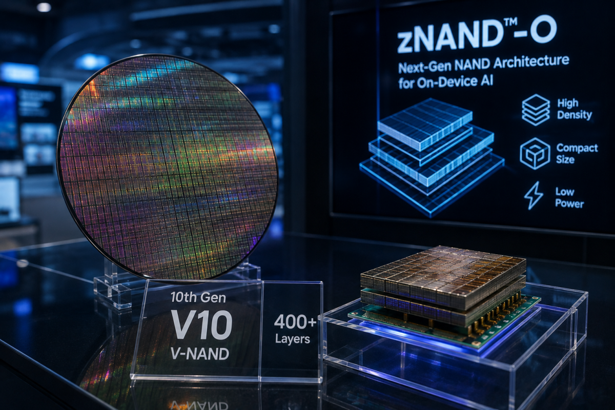
Samsung also introduced zNAND-O, a next-generation NAND architecture designed for on-device and edge AI. The technology combines layered NAND flash with multi-chip bonding to increase storage density while reducing physical size.
The company unveiled its 10th-generation V10 BV-NAND, featuring more than 400 memory layers—the first NAND architecture to surpass that milestone. Samsung said the new wafer-bonding design improves storage density by about 58% compared with the previous-generation V9 NAND while also enhancing read, write, and input/output performance.
Expanding AI Memory Portfolio
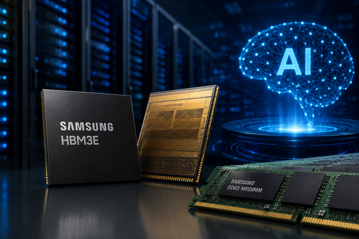
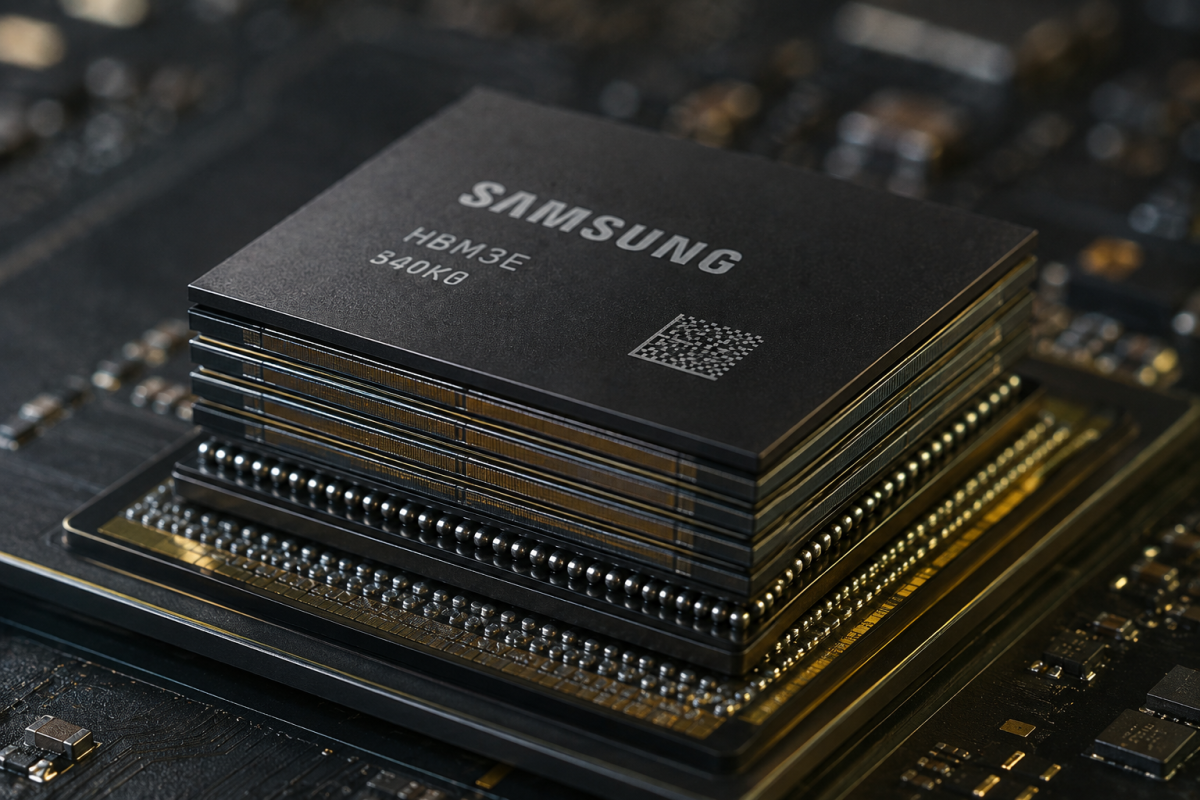
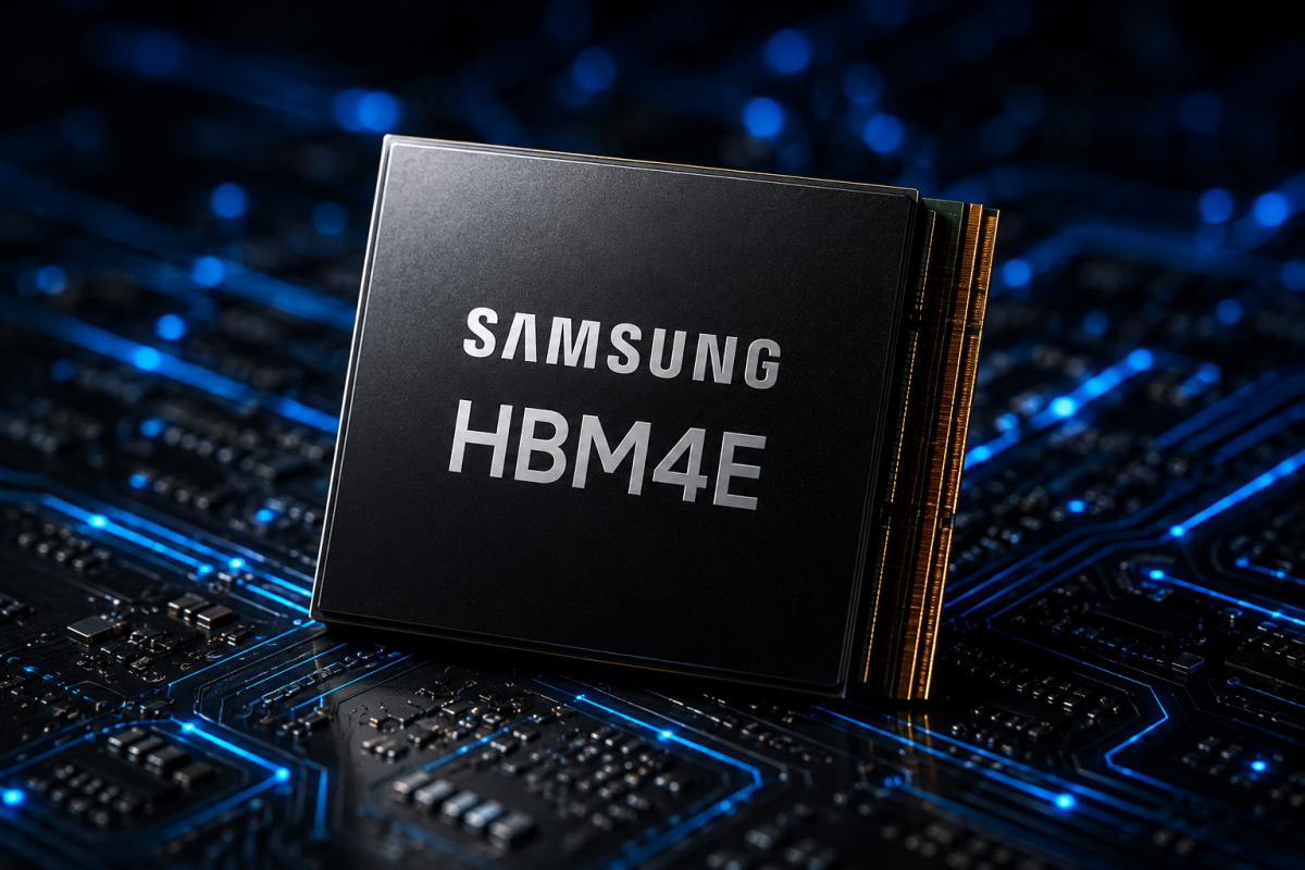
Alongside the new concepts, Samsung showcased HBM4E, a concept version of HBM5, LPDDR5X-PIM, and enterprise storage products for AI data centers.
Samsung said it became the first company to begin mass production of HBM4 in February 2026 and started shipping HBM4E samples to customers in May.
According to Counterpoint Research, Samsung currently leads the global DRAM market with an estimated 39% share, ahead of SK hynix (26%), Micron (25%), and CXMT (7%).
Why It Matters
As AI workloads continue to expand, advanced memory is becoming just as important as processing power. Samsung's latest announcements highlight the industry's growing focus on faster, denser, and more energy-efficient memory technologies that could help power the next generation of AI data centers, edge devices, and high-performance computing systems.